
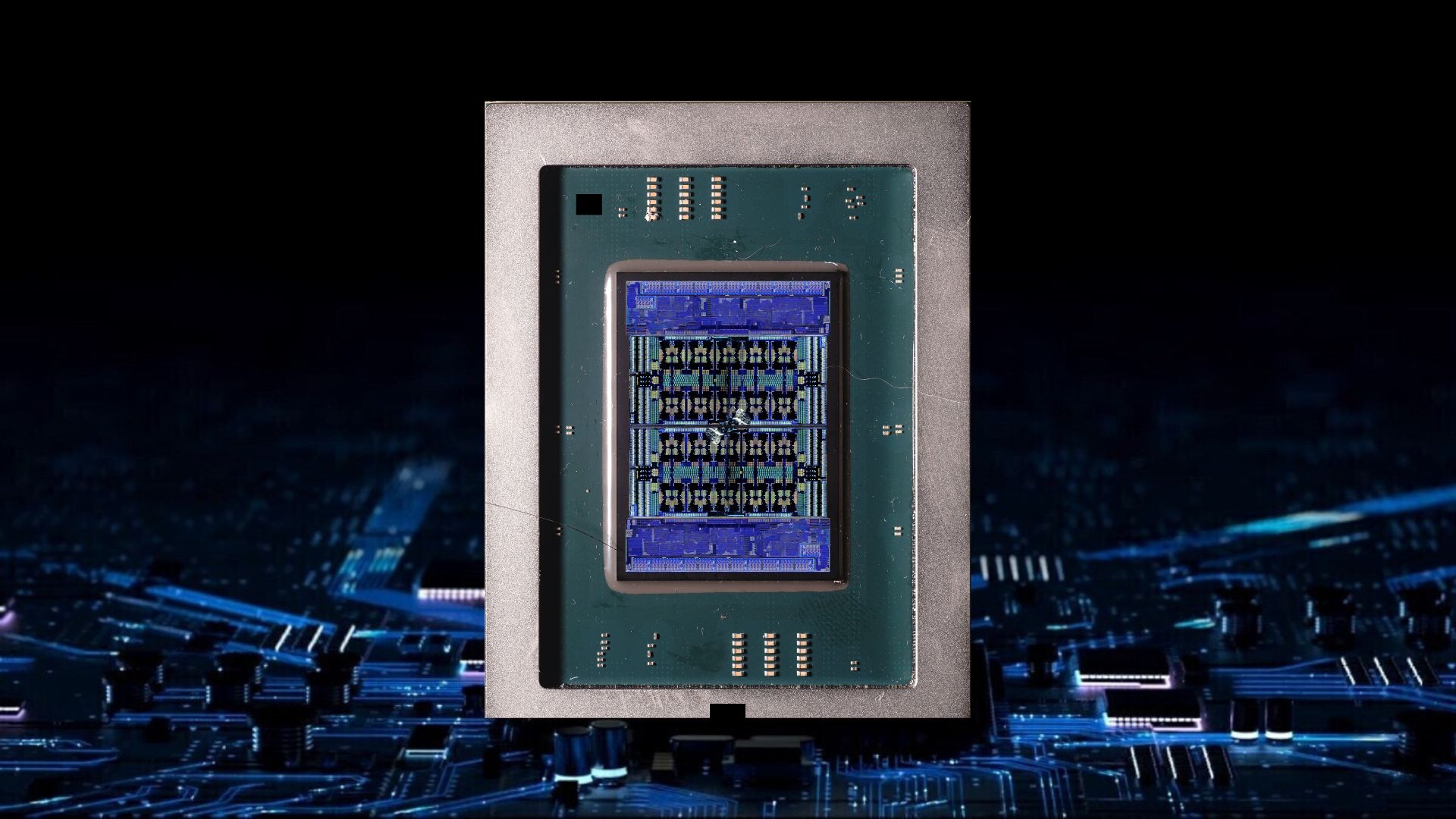
Huawei has taken a bold step forward in server computing with the debut of the Huawei Kunpeng 930, a chip revealed through a detailed teardown video that confirmed its foundation on TSMC’s 5nm process. This advanced design positions the Kunpeng 930 as a powerful upgrade, delivering almost double the performance of its predecessor while moving closer to the capabilities of global rivals like Intel and AMD.
The Huawei Kunpeng 930 combines a CPU built on TSMC’s N5 architecture with an I/O die reportedly fabricated on SMIC’s 14nm process. Measuring 77.5mm by 58.0mm, the chip is designed for dual-socket motherboards and incorporates Huawei’s Mount TaiShan CPU architecture. Each die integrates 10 CPU clusters, with each cluster housing two cores, bringing the total to an impressive 80 cores.
Performance gains are supported by advanced memory and connectivity features. Each die includes 91MB of L3 cache and 2MB of L2 cache, alongside 96 PCIe lanes and a 16-channel memory controller. These specifications highlight Huawei’s effort to balance raw computing power with bandwidth and efficiency, key elements for high-performance data center applications.
While the Kunpeng 930 narrows the performance gap with Western offerings, it still lags a few generations behind the latest Intel and AMD chips, which are moving into 3nm and 2nm territory. However, the use of TSMC’s 5nm node represents a breakthrough for Huawei, especially as it navigates ongoing technology restrictions and global semiconductor competition.
For industries requiring scalable computing, high-density workloads, and energy efficiency, the Huawei Kunpeng 930 signals that the company is determined to remain a serious player in the global server market.


